
Well, I tweaked the PCB design 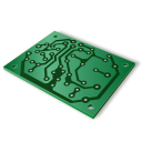 just a little more. Actually, very little—I was just seeing if there was a way to handle the
 USB  traces since these two NETs were 170mm and had a lot of vias. The center already had the other components and trace routing, so I guess there wasn’t much to do. And honestly, I’m not experienced, so I don’t know how to make these things better.
Along with that, there’s roughly an idea of how the project case will look and the items I had already been working on. 


Comments 0
No comments yet. Be the first!
Sign in to join the conversation.